


A Hardware Designer's Notes (Ramblings) on PCB Design and Testing

As Blue Clover Device's hardware designer, I get a lot of requests and questions from the team, as well as clients, for projects and explanations.
One recent humdinger from our marketing manager: “Hey, could you write a blog post on good PCB design practices for manufacturability, production and reliability?”
I’m always happy to help, but I was unsure as to how, or if, I could pull it off.
The internet is so full of easily searchable information on PCB design, that I doubted myself and the significance of a possible contribution, and seriously wondered if there was anything I could offer to other PCB designers.
“OK”, I thought to myself. “What are the main things I worry about when I design the types of PCBs I work on?”. “What do my checklists look like? What kinds of little loops run in my head while I'm laying out a board? How can I quantify and justify the artistic, intuitive and perhaps bizarre aspects of what I do? What design practices have I picked up from my experience working in research, start-up environments and now at an ODM?” Most importantly, “What have I learned over a modest hardware engineering career of incredible success and equally fantastical @#$! ups?”
First pro-tip: Ask yourself questions. Start an internal dialog. Just try to keep it in your head and don’t vocalize it, as people find that annoying.
Now that that’s out of the way, let’s talk PCBA design! In this blog post, I'll cover the following:
- A History of PCBs
- Schematics
- BOM
- Board Layout
- Board Size, Shape, and Part Placement
- Stackup
- Board Design Practices
- Design Rule Check
- Vias
- Decoupling (or Bypass) Capacitors
- Return Paths
- Analog/Digital Mixed Signal Design
- Prototyping
- Test Points and ICT
- Mounting Holes
- Test Points
1. History of PCBs
As a millenial, PCBs have always been a part of my life. From the first TV remote I took apart to building and repairing PCs with my dad as a kid, green circuit boards with a mix of through-hole and SMT were already in every consumer electronics device on the market. Although PCB and IC technology has advanced tremendously since then, to an untrained eye, PCBs and motherboards from the late mid to late 90s look the same as they do now. The basic PCB design/manufacturing principles and methodology is still the same for most consumer electronics. However, we design PCBs atop the shoulders of giants. At our disposal we have about 100 years of development of this technology, from the first patents in the early 1900’s, to the first mass produced PCBs in the 1950s for personal radios, to the development of the RS-274 Gerber standard developed in the 1970s, which is still (more or less) used today.
As much as I would love to write an entire blog series on the history of PCB design and manufacturing, it would be a deviation from my official mandate, and beyond the scope of this semi-educational blog… though I do encourage you to check out the following links as a primer to all of this:
https://www.pcb-solutions.com/pcb-market-monitor/the-history-of-pcb-infographic/
https://www.autodesk.com/products/eagle/blog/history-of-pcbs/
https://www.youtube.com/watch?v=J0ggqY7vnAw
“Open your mind to the past. Art, history, philosophy...and all this will mean something” - Capt. Jean Luc Picard
2. Schematic
Before one considers designing a PCB, one first needs to design and finalize a schematic. It is so important in fact, that all modern PCB design software requires a schematic to be completed (well, at least started). This is so the software can convert the wires in your schematic into ‘nets’, which is a set of minimum point to point connections that is equivalent to the human-friendly schematic. This is how the software knows what components need to be connected to each other on the PCB. Besides the simple connections, here is where you define the nature of those connections. For example, a connection providing power to a component may require wider traces and larger/more vias than a connection for a low voltage signal. It is always good practice to define your connections here, so you don’t accidently route a 6mil trace to provide 3A of power to your high power LED. Often you can define individual connections, or define classes of connection properties and assign them to individual connections. Differential pairs, controlled impedances, busses, power and grounds are also defined in the schematic.
Analysis and simulation are a big part of electrical design, and there are many tools available, ranging from integrated tools in your schematic/pcb software, free tools based on SPICE, to proprietary tools for simulating microcontrollers (although I would never recommend completely relying on MCU simulations for your designs. One would be better off purchasing a demo board). One of my favorite free tools when designing specialized analog or other functional circuits with discrete components is:
https://www.falstad.com/circuit/
It may be dated and a little crude, but the fundamentals are there and you can easily save and share designs with no pay-wall, sign-ups or other nonsense.
3. BOM
Ok, so once your schematic is designed, or perhaps before it is finalized, it is important to at least start thinking about your BOM. There are a few things to consider before selecting specific part numbers and packages:
Does the pitch of your component match the design rules of your chosen manufacturer? If you are doing a 6/6 or even a 4/4 board, you may still be using packages that have a pitch smaller than this.
Are you assembling this PCBA yourself by hand and not using a pick-and-place? Are you going to be doing some board level modifications (soldering/desoldering components) yourself? If so, what package can you comfortably work with? Most people can handle an 0603 package with a bit of training. Personally I can solder 0201 packages without any microscope or lenses, and can even do 01005 if I have to (hopefully I have a microscope to at least inspect my work). However I would still try to avoid using too many of those tiny packages if I knew I was assembling an entire 50+ part prototype myself. BGA components are also possible by hand, but are tricky to do, and impossible to inspect without some kind of xray machine. Also once you start using BGAs, you may have to incorporate micro vias and blind vias, which makes the PCB more expensive to manufacture. Sometimes however, you don’t have a choice, and require a BGA component.
One big factor for me these days is whether the part’s eCAD library exists online. Defining landings for packages and tying them to symbols is an arduous task. If you are not picky about the part number that is needed for the BOM, such as an LDO for a specific voltage, search to see if there is a part library that is available that fits your requirements on one of the following 3 sites:
https://www.ultralibrarian.com/
http://componentsearchengine.com/
Of course it is always good practice to verify that the library is correct before you use it.
Some other useful resources for BOM selection (and even schematic capture) are tools like Texas Instrument’s WEBENCH and Murata’s simsurfing tool. On WEBENCH you can select design parameters for your circuit, and it will suggest ICs that fit your requirements. Not only that, it will generate entire schematic reference designs for that specific IC and your set parameters, and recommend an entire BOM (one engineer I have worked with interestingly called the group of discrete components in a reference design ‘popcorn’). Not only that, you can also download the entire schematic straight into your eCAD software (it supports a few different platforms).
Murata’s SimSurfing tool allows you to enter electrical parameters for passive components, and view highly accurate data and characteristic plots on those components. It is much easier than trawling through hundreds of datasheets, while looking for that special component. However, you are stuck with Murata (which isn’t a bad thing, they produce high quality components imho).
Lastly before deciding on a component, it is important to see if it is an active component and widely available. Believe it or not, many quick turn manufacturers, even in China, require that the part number is available on popular US distributors like Digikey or Mouser. Many of them will order parts from there despite being on the other side of the Pacific. This is due to the convenience of their service (quick shipping, nice search interface, digi-reel service), and because having a backup reduces the risk of not sourcing the component locally. Also, if many distributors are carrying the part, it is less likely that the part will become obsolete. Obsolescence sucks.
A site like https://www.findchips.com/ is a great place to do this kind of search. Fun fact, findchips is owned by supplyframe, wich also owns hackaday and tindie! Their office is really close to ours here in San Francisco.
4. Board Layout
So you have your schematic and BOM compete. Now it’s time for the fun part. Simply place your components on your board wherever they fit and run the auto-router. Done. Wasn’t that easy?
.
.
.
Did you really think I was going to suggest that you use the auto-router to completely route your board? Seriously. I’m glad you are still here actually. I would have likely stopped reading already. If you are new to PCB design, then let me clarify: do not use an auto router. Route your boards yourself. Auto-routers are becoming really great, and eventually we will get to the point where an auto-router is able to route a board completely. But we are not quite there yet. There are at least 100 different rules of thumb that you follow when laying out a board, and some very important decisions that need to be made constantly that only come from experience (@#$#ing up). I’ll try to cover as much as I can here, but you should do some extra research!
Now that we have cleared that up, let’s continue with our board layout.
Explanation of what I am doing when curious co-workers look at my monitor: You have to trace 800 point to point connections, 8 layers, no connection can intersect. Go!
A) Board Size, Shape, and Part Placement
Sometimes your design is driven by the mechanical design or industrial design alone...But Hopefully the product design team consulted you, the hardware engineer, before the final size requirements were established. In this consultation, you did a schematic, selected your components, and roughly laid them out on the proposed PCB shape. Things were tight, so you decreased the package size of the resistors, capacitors (where possible!) and ICs. You went from 6/6mil trace width/spacing to 4/4mil. In your head you knew things would work, and if not, you have the luxury of adding layers and blind/buried vias. You report back to the product design team and give the green light. When management is ready to proceed, everything will be smooth sailing.
Unfortunately the above scenario would be ideal. It is not always the case. I have worked for hardware startups where the electronics were an afterthought. Seriously. They raised a bunch of capital or got upper management excited for a sexy, small widget. They designed the mechanicals, the look, the feel. Then they turn to a hardware engineer (sometimes on contract, never involved until this point) and they say, "OK, time for you to design us our electronics to fit in this thing, with A-Z functionality."
Now of course, anything is possible with the right amount of imagination, intelligence and most importantly, budget. I am going to assume that if you are reading this blog, developing your own purpose built microscopic ASIC using the latest and greatest technology is out of the question. In that case, you are limited to off the shelf components, and the PCB manufacturing capabilities of your prefered board manufacturer.
If your board size/shape is already determined for you (or if its not):
- Place all connectors that need to be in specific locations.
- Lay out all components, starting off with functional circuits, grouping circuits together based on power, then communication/signal requirements
- Group all circuits together in the proposed board layout, top and bottom (if the design permits.
If the components do not not fit, then it is time to consider reducing the package size of your components. Ensure that all components are SMT, as they require less real estate. Keep in mind, that reducing resistor packages means that the power rating will most likely also go down. Ensure that your new resistors are still sufficient. Also, capacitors come in all packages. The smaller the package, the lower the voltage rating. Also, the real capacitance at the application voltage/frequency may be much lower. Check the datasheets, especially the DC Bias and Frequency Characteristic charts. Also take into account your personal re-work limitations. Going down to a 0201 or an 01005 packages saves acres and acres of board real estate...but can you rework them with your soldering skills and equipment?
Try steps 1-3 again. If they still don’t fit, then here is where you need to start modifying the PCB design parameters. Starting from the least expensive to the most expensive changes:
- Shrink the trace width/spacing minimums. Most of my boards start off as 6/6mil trace width/spacing. 4/4mil design rules can actually free up a lot of space. Check to make sure your manufacturer can handle this. Also, what thickness do your power traces need to really be? I use online trace width calculators to determine the minimum trace width based on the application current. 4pcb’s trace width calculator is usually my go to: https://www.4pcb.com/trace-width-calculator.html.
- Reduce the via annular ring and drill size. Once again, check your PCB manufacturer, and second, check to make sure that your application can handle this. Vias are a little more tricky to calculate, as the inner diameter plating thickness of holes and vias isn’t as well controlled. The inner plating thickness determines the maximum current that via can handle. In the end however, a smaller via frees up even more space. http://circuitcalculator.com/wordpress/2006/03/12/pcb-via-calculator/
- Blind/buried vias. Now we are getting into some serious PCB design territory. But your board still does not have enough space, and you need more room dammit. Up until now, we have used through hole vias. A single through-hole via, regardless of its layer, punches a hole through the entire board. This is the cheapest way to produce vias on a multi-layered board. Check with your manufacturer to see if they can handle these. But if they can, then you will free up even more space.
- Vias in pads. This is another trick that can save a lot of space...but you simply cannot put vias in pads. This is because the via will drain the solder during the reflow process, leaving little to no solder for the part that is actually supposed to be soldered. If you go this route, the manufacturer will charge you more because these holes need to be plugged before the boards are pasted and populated.
- Layers. Lastly you can always increase the layers of your board. I’ll give my two cents on this later on.
B) Stackup
The second decision is how many layers. Really this decision should be binary. That is, can you accomplish the design with just two layers, or do you need multiple? The reason I suggest multiple, and not 4, 6, 8 etc, is that in my opinion, a hardware engineer should not limit oneself to a fixed layer count. Does a software engineer designing apple or android apps kick off their design by saying “This app will be less than X mb”? Do they limit themselves by a targeted file size? Not really, only to the extent that a large file size would be unreasonable (2GB for a simple chat app would raise a few eyebrows). Also, a good software engineer just does things efficiently to begin with. Like in software, arbitrary limitations in your hardware requirements can turn the design process into a game of making unnecessary compromises. In the end, your design will suffer for no good reason. For complex designs, less layers means more vias, less isolation, breaking up more ground planes/power planes, strange return loops, noise, poor thermal properties. The list goes on.
I am not aware of any quantitative formula to estimate a layer count. I guess such a function could be formulated based on connections (airwires), total landing surface area, board area, power requirements, isolation requirements, number of high speed signals etc...It would be a nice add on to a PCB layout software package.
Be cautious, however. Assuming that the inner layers of your board are used for ground and power planes, you will not have access to your traces if you go up to 6+ layers. For debugging this can complicate things.
In short, do not let the project manager or bean counter tell you that a board’s layer count should be limited. The layer count for your design is however many layers is necessary to fulfil your design requirements reliably and efficiently.
5. Board Design Practices
In this section, we are going to go over some more tangible rules of thumb and best practices that you should consider when designing a board. I can’t possibly cover everything here, but these are the points that come to mind.
We have all been confronted with a board, on the bench, all hooked up and not blinking. There was quite a bit of back-and-forth with the manufacturer and changes were made. But thankfully those changes didn’t affect the board. Usually the fix is simple, and you can quickly correct it. You run the board through a myriad of tests. Your bench testing is limited due to a lack of equipment, experience or expertise. Field testing is going great however, and the board is in production. Now that it has been deployed, issues start to pop up. The MCU hangs sometimes, forcing a hard reset. Some boards lose power and you don’t know why. Wireless communication is not so reliable, and inefficient communication redundancies, handshaking, extra acknowledgements need to be added in the firmware.
Of course with the right testing regimen, you would have been able to test for sources of noise, and how that is affecting your board’s functions. You could have used some thermal couples or infrared cameras to see how hot things were getting. You could have hooked the board’s PCB antenna to a network analyzer and tested the antenna’s efficiency. But you didn’t have the time, budget, equipment or experience doing so.
All that being said, you would have caught those issues, and would have likely needed to do a design revision or a complete redesign.
The thing about PCB design is that it is usually not a single issue that affects reliability. Often one or two lapses in design judgement won’t break things. However multiple issues stack up and start to insidiously affect reliability. Sometimes these issues cause physical manufacturing errors, while some issues can be purely electrical. Having a solid set of design practices can help you reduce the probability of errors, and assist you in designing cleaner and more reliable boards. Designing a board to power up and show some semblance of life is easy enough. The real challenge is designing a board that is reliable is a whole other ball game.
A) Design Rule Check
First and foremost, it is important to input your manufacturer’s design rules into your layout software. Some manufacturers actually have design rule files for multiple eCAD packages. On most eCAD software, you will be instantly updated if you do something that is out of spec, such as clearances, thicknesses, drills etc. Properly setting up your design rules before you start the layout process is crucial to your personal design efficiency and reliability of your board.
Further, you should run your design rule check before your board is submitted to your manufacturer. Do not ignore any warnings. Dig into why each error is flagged. Do not leave anything to chance. I cannot stress this enough!
B) Vias
I touched on vias already, but there is so much more to be covered.
There are 3 main types of vias. Through hole, buried and blind. There are also micro-vias, which are defined as plated holes, with an aspect ratio (diameter:depth) of 1:1 or less, and a diameter of 0.25mm (9.8mil). However this is an IPC standard, (originally called the ‘Institute of Printed Circuits’, now IPC calls itself ‘Association for Connecting Electronics Industries’ ) and manufacturers will have their own definition of what they consider micro-vias. The aspect ratio makes sense, as when the smaller and longer the hole, the trickier it is to drill/laser it reliably. Microvias and blind/buried vias are necessary for some larger, finely pitch BGA packages. If you are trying to free up board real estate, buried or blind vias can be very helpful, but beware of the extra costs.
Also we already talked about vias-in-pad. Usually manufacturers will charge extra to plug them up to prevent soldering defects. However, some manufacturers will not be bothered if you don’t specify via-in-pad requirements, and will solder your board, ignoring your pads. This may lead to defects.
You need to seperate vias sufficiently from your pads for the above reasons. A via too close to the pad (inside of the pad’s solder mask stop) will cause the solder to drain through the trace, into the via, and take away solder from your pad.
Lastly, whenever a batch of your boards is produced, it is nice to ensure that the plating of your visa are consistent. You can either ask the manufacturer to place a sacrificial via on your board, or you place it yourself. When the boards are produced, the manufacturer can slice vertically through the via and inspect the plating thickness and consistency. Flying probe or other electrical tests are often provided as a service by the PCB manufacturer. These electrical tests are based on your gerbers, and they are usually just testing for continuity. Poorly or thinly plated vias will not be caught however, and can pose serious problems with current and signal integrity.
C) Decoupling (or Bypass) Capacitors
The great thing about downright microscopic, high frequency digital circuitry and tiny, high power switching power supplies, is that we can pack a great deal of functionality into a tiny, efficient package. The downside is that these circuits are incredibly noisy and the power fluxuates. So much so, that almost all analog and digital chip manufacturers recommend some kind of decoupling in the form of capacitors placed on every power input.
You would think that if the manufacturer devoted a reference design and a paragraph to decoupling capacitors in the datasheet, engineers would take this seriously and design their circuits/layout accordingly. In my experience, decoupling is the first thing engineers will compromise on when miniaturizing their boards. Or they will downright not do it, or do it incorrectly. This is due to many factors, such as previous experience ‘getting away with it’, a lack of understanding of the reasons and principle of decoupling, and a disconnect between a simple passive component and its effect on overall performance.
This ties back into the idea that we have already discussed, the idea of a multitude of smaller compromises and poor design choices chipping away at your board’s overall reliability. Good decoupling discipline will make your boards more reliable and work as intended.
What does a decoupling capacitor do? It’s main functionality is to act as a device’s local backup energy reservoir, and to act as a low impedance path to ground for AC and noisy signals on the DC power rail. Power can fluctuate for two main reasons on your PCB. First, the device you are decoupling (or others on your board) may intermittently draw relatively high amounts of power (like a transceiver or MCU), dropping or raising the voltage temporarily while the switching power supply’s feedback circuitry compensates. If we have a decoupling capacitor nearby, the capacitor will discharge into your device when the voltage drops, or charge when the voltage spikes, providing a more constant voltage level for your device, thus reducing noise. Second, a switching power supply introduces periodic and semi-periodic noise on your power line. This can’t really be helped, as the switching effect is fundamental to the power supply’s operation.
As a rule of thumb, it is wise to select larger capacitors (~10uF) for lower frequency noise (tantalum or electrolytic). This will help smooth out larger fluctuations and intermittent power transients, providing a more stable voltage for longer periods. Lower capacitance values (0.001-0.1uF) are better suited for higher frequencies.
Since no capacitor is ideal, a capacitor will have an equivalent series resistance (ESR) and equivalent series inductance (ESL). Because of this, capacitors will have a self resonant frequency (SRF). This is really handy, because you can select a capacitor based on its SRF to target ( or ‘short’, but not really because of a low ESR) specific frequencies, or select an array of capacitors to deal with an entire band of frequencies.
Lastly, you need to place your capacitors as close as possible to the power input of the IC. When the IC is relying on the capacitor as a power reservoir, it is important that we are mitigating other ill effects that would detriment the bypass circuit. Longer traces between your capacitor and IC can introduce impedance and parasitic inductances and prevent the decoupling capacitor from doing its job. Many ICs are designed with ground pins close to the power pins. You use this configuration to help decouple the IC, by placing both ends of the capacitor as close as possible to Vin and GND (don’t forget that GND is simply a negative return, and that current passes from the GND pin to the board’s GND. You will still introduce impedances and parasitic inductances if the Vin path is short but the GND path is still long).
No matter how you decide to use decoupling capacitors, always read the datasheet’s recommendations first.
D) Return Paths
Speaking of return paths, this is another thing that must be considered before you manufacture your board. Basically the current of any circuit will take the path of least impedance to GND. You must keep this in mind when routing your board. Examine how a signal or power rail’s current will find its way to the GND. Most likely this current will travel through an IC or a passive component. A designer strives to keep this distance as short, and as little impedance as possible with the use of ground pours and multiple vias to the ground plane. When a ground pour is used on a signal layer, it is important to examine how the ground pour is segmented and broken by other races. Often you may find that, although your software recognizes that something is grounded, the resulting ground pour may be such that the path to GND is but a tiny piece of copper that cannot hold any significant current and is of high impedance. Some DRCs will allow you to check for this.
There are a few consequences of having poor return paths.
- Currents will flow to parts of your board that are unintended
- You may unintentionally generate large amounts electro-magnetic interference
- You increase the chances of cross-talk and noise
- Poor thermal dissipation
- Heat generation from high impedance traces
- Lower efficiency and malfunctions due to added impedances to return paths.
In short, always create a separate GND trace for a part with a wide trace and via to the GND plane. If you are designing a 2-layer board, ensure that there are ample low impedance paths to GND. Use a technique called ‘via-stitching’ to catch stray currents before they travel all over your board. For 4-layer boards, examine the ground plane to make sure there is not any unintended segmentation by non-GND throughhole vias.
These are the basic steps that can be taken, but there is a plethora of info on designing cleaner boards and reducing return paths. Google is your friend!
E) Analog/Digital Mixed Signal Design
Hopefully our above discussion so far has inspired a new perspective when routing a board. When you think of your PCB as multiple smaller circuits that all eventually return to GND, you design cleaner, more efficient PCBs that have less noise, and less problems.
Understanding return paths also makes it easier to understand mixed-signal design.
Analog sensors are not going away. The nature of an analog sensor gives it potentially infinite resolution and precision due to its continuous nature. To get the most resolution out of an analog sensor, you need to separate the analog components from the digital components. As we discussed, digital circuits are extremely noisy. Switching power supplies, digital signals, MCUs, all connected to GND, and its noisy current traveling through it. For an analog sensor, this digital noise would wreak havoc. To use an analog sensor, its voltage needs to be measured for the smallest changes.
In order to mitigate the digital noise issue when designing PCBs that require both digital and analog circuitry (mixed-signal design), the circuitry is kept seperate. This will entail using separate power supplies (LDOs vs switching power supplies), lots of filtering and decoupling, and most importantly separate GND planes for the analog side of the board.
It is inevitable that some digital signals will need to travel to the analog side and vice versa. However, from our discussion of return paths, hopefully you can see a way that we can keep the ground planes separated enough, while allowing for some signals to pass through without contaminating the sanctity of the AGND.
There are many design practices involved in doing this correctly, and once again, there is so much information online. I’ll point you to a good introductory article on the subject that demonstrates some techniques.
http://www.hottconsultants.com/pdf_files/june2001pcd_mixedsignal.pdf
6. Prototyping
Trace Modification and Debugging
When designing a prototype, there are always some unknowns. The problem with a PCB is that we cannot easily make corrections to the design once the board is fabricated. There are a few techniques that can be used to make your debugging experience easier when testing your prototype.
- Design traces such that they can be cut with a scalpel. We all love multiple traces packed together, traveling in unison from one side of the board to the other. However if you are designing this with 4mil traces, it can be incredibly difficult to cut a single trace and jump it elsewhere. Make sure that each trace has the space required for it to be cut, for the solder mask to be scraped, and for it to be soldered.
- Use solder jumpers. Put them on anything you are not sure about. Better to have them and not need them, then need them and not have them.
- Use 0-OHM resistors on every major circuit, especially power supplies. This is a really good trick to help with the debugging process. Simply desolder the resistor when trying to figure out what is going on with your PCB.
- If your trace is primarily on an internal layer, make sure there is a way for you to cut it off and re-route it. If the signal allows for it, pop it up to an external layer somewhere on the board.
- If an IC does not have exposed leads, create exposed pads that are directly connected to pins that you are unsure about.
- Create an area on your board that you can use to connect to your test equipment.
- Add many test points.
If you take the above steps into consideration, you will save yourself money and time, guaranteed.
7. Test Points and ICT
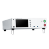
In this section we are going to talk about test points and ICT (In Circuit Testing). In the PCB design world, test point design is what separates the boys from the men. Properly sized and spaced test points shows the world A) my board is going to be produced in volume, B) every circuit on every board produced is going to be verified and tested to my rigorous design requirements, and C) the designer is professional, experienced and seasoned enough to know how to use test points.
It just so happens that I am employed by the world’s largest quick-turn ICT manufacturer, with our very own product dedicated to testing PCBs. Much of what I am going to suggest for test point and pogo pin design is specific to our products, however, is just good practice in general.
A) Mounting Holes
Most likely your board will need these so it can be placed in an enclosure. This is not always the case however, as your design may be potted, press fit, epoxied, glued or slotted into your design.
If you are using mounting holes, they will most definitely be used for when your board undergoes ICT testing. If this is the case, please consider the following:
- Leave your holes unplated, as plating the holes will decrease the hole diameter in an unpredictable way. The locating pins on your ICT fixture may not fit, and the board will sit too high for proper pogo pin and press plate function.
- Use standard PCB mounting hole sizes. Standard imperial sizes are 0.062”, 0.093”, and 0.125”. Common metric sizes are 1-3mm, in 0.5mm increments. This makes it easier to source your mounting pins, and reduces tooling costs for your manufacturer (costs that are passed onto you)
- Place your mounting holes at the outer edge of the board, and ensure that the board is ‘balanced’. If you are using only 2 holes on one side of the board, how will it remain stable when it is sitting on the locating pins, or being pressed by the press plate? This creates problems for the ICT fixture designer, and once again, will raise costs.
- If you are using your mounting holes for metallic screws, please keep them away from antennas! Metal in close proximity will most likely detune the antenna, reducing the antennas performance.
- If a plated mounting hole must be used, then do not rely on it for ICT fixture mounting.
- Leave 4mm space (center to center) between mounting holes and pogo pins.
B) Test Points
ICT aside, test points are incredibly useful for debugging and testing your PCB on the bench. Ideally, all signals and power traces on your board will have a corresponding test point. This in turn makes any modification much easier, as any point can be soldered together with the use of jumpers.
First, for those who are not familiar with test points and their uses, let’s discuss how they work and how they are used.
Top to Bottom: Pogo Pin Test Points, Through Hole Test Points, and SMT Test Points
The above images show the different kinds of test points. When people talk about test points, they can be describing any of the above images. For the purpose of this discussion with regard to ICT, we are referring to test points designed for pogo pins.
When designing a board with test points for pogo pins, we are assuming that an array of probes will contact the test points from the bottom of the board. These probes will either provide power, enable communication, or test the electrical characteristics of the circuit (impedance, voltage, current, frequency etc).
There are multiple types of tips that can be used on the probe:
Different types of pogo pin tips
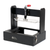
In general, we support the following ‘Design Rules’ to be implemented on your PCB (design under test, your PCB) for our pogo pin cassettes https://www.bcdevices.com/product/ppc/
These rules are good design practices in general, and would make any ICT fixture designer’s life a lot easier:
- Make sure that the pogo pins have at least 2mm clearance from other pogo pins. We use S-075 pogo pins (1mm diameter) for the most part. Smaller pins are certainly available, however placing, drilling and aligning these smaller pins pins are quite difficult, and are not as mechanically reliable in a production environment.
- The test point should have a 1mm diameter. If the test point is smaller than this, misalignment may occur.
- Place a test point for all through hole pads. You can’t easily use a soldered through hole pad as a test point on an ICT fixture. Sure, there are cupped tips available, and techniques that have been developed. You would also have to make sure that the leads of the through hole components are a fixed length, and that the solder is controlled to reduce variability in the shape. It’s just easier for everyone if you make a seperate test point.
- Place a test point for all connector pins. It is a common misconception that ICT designers can simply use the PCBs connector for testing. Although it is possible to connect a board manually, or incorporate the mating connector on your fixture, this just adds time and cost to the ICT fixture build.
- If you are supplying higher current to your DUT, make sure the pogo pin can handle the current. Our S075 pogos are rated for 3A, however it is good practice to design for half of that. To keep things simple, use multiple test points on the same trace to deliver higher currents
- Allow 0.2mm (8mil) spacing between the test point and any trace. This is due to alignment. If the pogo misaligns, it may puncture the solder mask and create shorts, damaging your board.
- Design a sufficient number GND test points. If your DUT requires a higher current, don’t forget that the negative return (GND) needs to handle that current as well. As a rule of thumb, add as many GND test points as PWR test points on your DUT.
- Place your GND test points in appropriate locations. Remember our discussion about return paths.
- Ensure that all traces to your test points are low impedance. Ensure that the trace to the test point is thick enough for the current that is passing through it.
- Through hole test points are great because you can use them from the top or bottom of your board, and it helps the pogo self-align. Ensure that the hole is centered.
- If you are going to place a via in a test point, ensure that it is centered. If not. it can cause misalignment of the pogo pin when it contacts the test point.
- Keep your test points away from any through hole solder pads. If there is not sufficient separation, solder may leak onto the test point creating a dome of solder on the test point. This obviously affects the alignment, as the pogo will be pushed to the outer edge of the test point.
- If your test points are on the bottom of the board, and your board is being wave soldered, ensure that the manufacturer masks your test points. Like in 10), your test point will become domed with solder.
- Spread out your test points, rather than concentrating them to a small area of the board. This allows for even pressure exerted by the pogos when the DUT is pressed.
- Keep your test points away from the edge of your PCB. If the pogo pin is misaligned, it will ride up along the edge of the board, damaging the pogo pin.
- Leave space on the top of your board or hold-down posts. It is not good practice to press down on the board on top of components.
- Somewhat hold-down post related, but important. If your board is going into production, it is important that you have a method of serializing your boards. Always leave a space on your board for this, whether it will be laser etched, stamped, or a stickered on. At BCD we offer pick-and-place compatible QR code or datamatrix stickers. You can add these as a BOM item to keep things simple. A hold-down post can press on these stickers, so the space does not totally go to waste.
With that, I conclude my notes (or maybe ramblings) on PCB design and testing. If there is anything that you would like me to talk about WRT PCB design or testing, or if there is something you would like me to elaborate on, please let me know at brien@bcdevices.com!
About the Author
Brien G. East Jr. is the Director of Hardware Engineering at Blue Clover Devices. A Canadian expat, Brien is happy to embrace sunny California as his new home.
Latest Stories at Blue Clover


Leave a comment